报告题目:New Materials and Devices Beyond Si CMOS
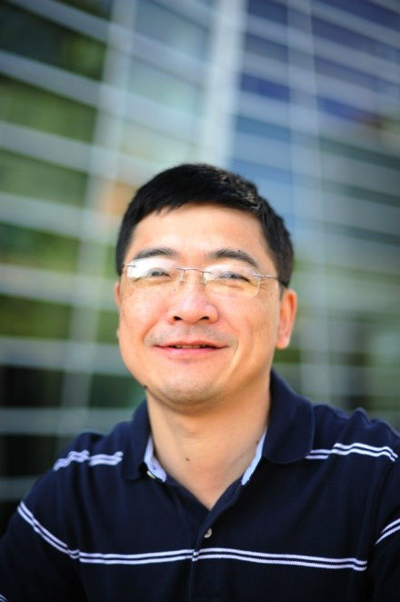
报告人: Prof. Peide D. Ye (叶培德)

School of Electrical and Computer Engineering
Purdue University
报告时间:2014年7月2日 下午2:30
报告地点:西区特种实验楼2楼阶梯教室
主办单位:微纳研究与制造中心
微尺度物质国家实验室
外办(港澳台办)
报告简介:
In the past decade, as scaling of Si CMOS technology approaches its end, III-V and Ge are indentified as the high-mobility channel materials to replace Si beyond 10 nm node according to the newest ITRS. The rise of two-dimensional (2D) atomic-layer crystals, such as graphene, MoS2 and phosphorene, has also given unique opportunities and challenges to the device research. In this talk, we will discuss the device perspective of these new materials and report on some of new breakthroughs on GaAs CMOS, Ge NFET, MoS2 FET, and few-layer phosphorene PFET.
报告人简介:
Dr. Peide Ye is a Professor of Electrical and Computer Engineering and University Faculty Scholar at Purdue University in USA. He received the B.S. from Fudan University, Shanghai, China, in 1988 and Ph.D. from Max-Planck-Institute of Solid State Research, Stuttgart, Germany, in 1996. Before joining Purdue faculty in 2005, he worked for NTT, NHMFL/Princeton University, and Bell Labs/Agere Systems. His current research is focused on ALD high-k integration on novel channel materials include III-V, Ge, CNTs and graphene, complex oxides, topological insulators, and layered 2D crystals. He authored and co-authored more than 250 peer reviewed articles and conference presentations. He is a Fellow of IEEE.
